XSPICE is a group of extensions to the SPICE3 simulator developed by the Georgia Tech Research Institute (GTRI). It enables you to:
- Perform simulation of event-driven and mixed-mode circuits. Mixed mode simulation is not limited to simulation of interconnected digital and analog circuits. It can simulate any kind of mixed-mode discrete-time/analog system. Discrete time signals can have more than 2 or 3 values (HI, LO and UNKNOWN) This depends on the type of the node whose value is the value of the signal. Beside digital, you can also have real (for simulation of floating-point DSP algorithms) or integer nodes (for simulation for fixed-point DSP algorithms). Of course various signal types can be converted among each other by using node bridges.
- Add new discrete time node types that can be loaded at runtime (1, 2) User Defined Nodes or UDNs - e.g. digital or real nodes
- Add new devices to SPICE (Code Models or CMs) that can be loaded at runtime. (1, 2) These devices can be either analog (e.g. Laplace s-domain block), event-driven (e.g. digital nand gate, z-domain delay) or hybrid (e.g. controlled digital oscillator, digital to analog node bridge)
- Digital nodes. A 3-state 4-strength digital node (UDN) is built-in into the simulator. An extensive code model .cm library is provided with SPICE OPUS for simulating digital circuits.
- Subcircuit expansion is now more intuitive and accessing internal nodes, devices and models of a subcircuit is now easier for the user.
- Dependent polynomial source support (SPICE 2g6) is included. The parser translates the SPICE2g6 syntax to a code model description of the source. This code model then simulates the source. (2)
- SIN, PULSE and SFFM transient sources now support an additional phase parameter. SFFM has now 2 phase parameters (for carrier and modulation).
- Capacitor an inductor code models that support initial conditions and supply ramping are included.
- Supply ramping for transient analysis is provided. At startup values for all independent current and voltage sources and initial conditions for capacitor and inductor code models are linearely ramped towards their final value at a rate which you define.
- Matrix conditioning. In case there is no DC path to the ground you can instruct the simulator to add a resistor with high resistance connected to ground at each node. This is of course the faster solution to the problem. But the better one is still the classical one: finding why the node has no path to ground and fixing the circuit appropriately.
- Gmin stepping and source stepping algorithms can be disabled separately. Improved control over DC analysis algorithms and mixed mode simulation is provided.
- Improved convergence problem reporting.
(*) Requires knowledge of C programming. Supported under Windows and Linux.
(**) Circuits containing CMs support AC, DC and transient analyses. AC analysis is not supported for circuits
with event-driven nodes.
Code models
XSPICE extends the basic SPICE functionality with code models (CMs). Code models are device models written in C and can be dynamically loaded into the simulator core. CMs can support the following analyses: OP, DC, TRAN and AC. CMs are not limited to analog models but can be purely event-driven (digital and gate) or hybrid (controlled digital oscillator or node bridges, e.g. analog-to-digital node bridge).
Event-driven simulation
In case your circuits contain no event-driven nodes (UDNs) nor event-driven code model instances (pure event-driven and hybrid CM instances) the event-driven simulator doesn't participate in the simulation and everything is done by the analog simulator.
Mixed mode simulation is used when your circuit contanins at least one event-driven CM instance. Event-driven algorithms work together with the analog simulator to produce results. Supported analyses for mixed-mode simulation are OP, DC and TRAN. Mixed-mode simulation and analog simulation are iteratively exchanged until event-driven outputs of event-driven CM instances stop changing.
Mixed mode simulation is implemented as "native mode". This means that the event driven simulator is implemented in the same executable as the analog simulator thus eliminating unneccesary overhad caused by the communication between both simulators that is typical of "glued mode" implementations.
In order to perform mixed-mode simulation you must have at least one mixed-mode CM instance in your circuit. Event-driven instances connect with their event-driven ports (inputs and outputs) to event-driven nodes. These nodes differ from analog nodes. They are implemented as User Defined Nodes (UDNs). UDNs can change their value only at discrete times. There can be many different UDNs in your circuit. A distinct UDN type has a predefined set of values. For instance a digital UDN (digital UDN is built-in into the simulator core) can have one of 3 logic levels combined with one of 4 logic strengths. The code that describes a certain UDN defines the way multiple conflicting outputs of different CM ports that are connected to the same UDN are resolved in order to produce the value for the UDN. Users can write their own UDNs in C and dynamically load them into the simulator core.
To connect the analog part of the circuit and the digital part of the circuit special hybrid CMs are used. These CMs are called node bridges. They translate one node type value into some other node type. For example to translate an analog node value into digital node value an analog-to-digital CM instance is used. For inverse translation you can use the digital-to-analog CM.
SPICE2g6 POLY sources
XSPICE supports SPICE2g6 polynomial controlled sources (POLY sources). They are impelemnted as CMs. You don't have to use the standard CM approach to adding a CM instance to your circuit. The translation from the SPICE2g6 syntax into XSPICE syntax is handled by the parser when the circuit is loaded. Polynomial source CM is built-in into the simulator core.
| Polynomial source type | Syntax |
|---|---|
| VCVS | Ename N+ N- (POLY (ND)) NC1+ NC1- .. NCND+ NCND- P0 (P1 ...) |
| CCCS | Fname N+ N- (POLY (ND)) Vname1 .. VnameND P0 (P1 ...) |
| VCCS | Gname N+ N- (POLY (ND)) NC1+ NC1- .. NCND+ NCND- P0 (P1 ...) |
| CCVS | Hname N+ N- (POLY (ND)) Vname1 .. VnameND P0 (P1 ...) |
In case ND=1 (one dimensional POLY source) POLY(1) may be ommited.
Arbitrary phase sources
Arbitrary phase is supported for the following transient sources: SIN, PULSE and SFFM:
| Transient source | Syntax |
|---|---|
| PULSE | PULSE (Vlevel1, Vlevel2, Delay, Rise_Time, Fall_Time, Pulse_Width, Period, Phase) |
| SIN | SIN (Voffset Vamplitude Frequency Delay_Time Damping_Coeff Phase) |
| SFFM | SFFM (Voffset Vamplitude Carrier_Frequency Modulation_Index Signal_Frequency Carrier_Phase Signal_Phase) |
Capacitor and inductor CMs
These CMs support initial conditions and supply ramping.
A1 1 0 cmodel
.MODEL cmodel capacitor(c=1000u ic=1)
A2 1 0 lmodel
.MODEL lmodel inductor(l=1m ic=0.05)
Supply ramping
Supply ramping is provided as an option to a transient analysis to simulate the turn on of power supplies. The values of all independent sources and initial conditions for capacitor and inductor CMs are ramped from 0 toward their final values in a time specified by user. To turn on the supply ramping option, use:
.options ramptime=RAMPING_TIME_IN_SECONDS
Matrix conditioning
In case an analog node has no DC path to the ground, the simulation doesn't converge and you get an error message. In order to make the circuit work you must find the node and provide a DC path to the ground (in most cases you would add a very large resistance between the problematic node and the ground node). XSPICE has the 'rshunt' option which does this for every analog node in the circuit. To turn on this option, use:
.options rshunt=RSHUNT_VALUE
You can use for example 1.0e12 for the rshunt value. In case you still have problems, try decresing the rshunt value gradualy to 1.0e9 or less. The best solution to the 'No DC path to the ground.' is still to find the node that is causing the problems and add only one 'rshunt' resistor manually to that node.
DC convergence options
The default convergence problem solving algorithm for DC analyses is GMIN stepping. If GMIN stepping fails, source stepping is used. In order to make the source stepping the default algorithm, set the gminsteps option to 0:
.options gminsteps=0
.options srcsteps=1000
This makes source stepping the default convergence problem solving algorithm. After 1000 source stepping steps the GMIN stepping is used. The 'maxopalter' option sets the maximum number of analog/event alternations. To set the maximum number of event iterations, use the 'maxevtiter' option.
.options maxopalter=1000
.options maxevtiter=2000
In order to enable the analog/event alternations, use:
.options noopalter=FALSE
To set relative and absolute step size limits applied to CM inputs in solving for the DC operating point:
.options convstep=0.01
.options convabsstep=1e-6
Code models, UDNs and .cm files
SPICE has a built-in set of device models (diode, BJT, MOS, ...) that can be used in your circuits. XSPICE enables you to create your own device models and use them in your circuits. You can write such a model (CM) in C.
Since XSPICE has an event-driven simulator built-in that is capable of simulating event driven circuits you can define your own event-driven node types. A digital node is built-in into the SPICE OPUS simulator but you can create also other event-driven node types. These node types are User Defined Node types (UDNs) and are also written in C.
In order to use the CMs and UDNs written in C in your circuits you must compile them and then load them into the simulator before loading your circuit that uses these CMs and UDNs. SPICE OPUS comes with a precompiled set of CMs and UDNs. Among those you can find integer and real UDNs, blocks for system level analog simulation, various digital gates and node bridges.
CMs and UDNs are stored in a .cm file that can be loaded into the simulator. In order to load a .cm file, type the following command in the NUTMEG prompt:
cmload filename.cm
Example:
Spice Opus 2 -> cmload analog.cm
analog.cm, version 1.0, Feb 25 2000
Analog system-level simulation library.
Author: GTRI, adapted by Arpad Buermen
Copyright: (c)2000 CACD Group, FE Ljubljana
Found 17 CM device(s) and 0 UDN(s).
Successfully loaded 17 CM device(s) and 0 UDN(s).
cmload searches for the .cm file in the SPICE lib/cm directory, in the system dll search path and in the current directory. The supplied .cm libraries are loaded at SPICE OPUS startup. The command that load these .cm files are in the spinit script provided with SPICE OPUS (lib/scripts):
cmload analog.cm
cmload digital.cm
cmload xtradev.cm
cmload xtraevt.cm
To see which analyses, UDNs and CMs are available at the moment use the siminfo command:
siminfo [analyses] [devices] [nodes] [all]
siminfo all
shows all simulator information.
Compiled CMs and UDNs are linked together with some header information and functions into a .cm file. A .cm file is actually a dll containing the compiled CMs and UDNs. Templates for creating .cm files are in the template/ directory. This directory contains template files for describing CMs and UDNs, .cm header .h and .c files and makefiles for Microsoft Visual C++ and Linux GCC that build the .cm files containing your CMs and UDNs.
As already mentioned XSPICE CMs can support DC, AC and transient analyses. SPICE OPUS supports all SPICE3 analyses for pure analog circuits without CMs. For pure analog circuits with one or more CMs SPICE OPUS supports OP, DC, AC and TRAN analyses. For mixed-mode circuits SPICE OPUS supports only OP, DC and TRAN analyses.
Introduction to Using Code Models in Circuits
Code models are marked with device letter A. Let's take a look at an example that uses the 'gain' code model:
Vin 1 0 DC 0 AC 0 SIN 0 2 50
A1 1 2 foo
.model foo gain(in_offset=0 out_offset=0.5 gain=2)
Rout 2 0 1k
'gain' is a CM for an amplifier with offset
out=gain*(in+in_offset)+out_offset (eq. 1)
In our case the 'gain' CM calculates the voltage for node 2 by taking the foltage
from node 1. Its input acts like a voltage probe at node 1 and its output as a voltage
source connected between node 2 and ground (node 0). The voltage for the output voltage
source is calculated from the input signal (in our case voltage at node 1) using
the equation (eq. 1) that was programmed in C, compiled and stored in the .cm file
(in our case analog.cm). This .cm file was loaded by the cmload command in in the
spinit script at SPICE OPUS startup.
There are 4 things you must know about code models:
- The device letter for code models is A.
- Code model instances have no instance parameters Instance parameters are parameters you provide on the line where the instance is described (in our case 'A1 1 2 foo'). A1 is in our case an instance of model 'foo' whose behaviour is described by the 'gain' code model and its parameter values. An example for an instance parameter is the resistance for a resistor.
- Code models have only model parameters Model parameters are given on a '.MODEL' line. In our case the model name is 'foo' and the code model to use for 'foo' is 'gain'. Values for model parameters for the 'foo' model are given in the .MODEL line.
- Code model instances can be connected with the rest of the circuit in many different ways. The allowed ways to connect a code model instance to the circuit are compiled in the code model. You can see them by inspecting the .ifs file for that specific code model. Details are described in the next two sections of this document. In our example we used the simplest possible way to connect the code model instance with the rest of the circuit.
Code Model Interface Specification (.ifs) File
The .ifs file is a part of the CM's source that describes its interface to the outside world. The CM itself is described in a .mod file. Usually you want to distribute the binary CM libraries (.cm files) that contain the compiled versions of CMs and the .ifs files for those CMs. The users can then quickly find out everything about the CM's interface from its .ifs file.
The .ifs file for the gain code model (gain.ifs) is as follows:
NAME_TABLE:
C_Function_Name: cm_gain
Spice_Model_Name: gain
Description: "A simple gain block"
PORT_TABLE:
Port_Name: in out
Description: "input" "output"
Direction: in out
Default_Type: v v
Allowed_Types: [v,vd,i,id,vnam] [v,vd,i,id]
Vector: no no
Vector_Bounds: - -
Null_Allowed: no no
PARAMETER_TABLE:
Parameter_Name: in_offset gain
Description: "input offset" "gain"
Data_Type: real real
Default_Value: 0.0 1.0
Limits: - -
Vector: no no
Vector_Bounds: - -
Null_Allowed: yes yes
PARAMETER_TABLE:
Parameter_Name: out_offset
Description: "output offset"
Data_Type: real
Default_Value: 0.0
Limits: -
Vector: no
Vector_Bounds: -
Null_Allowed: yes
.ifs files are not case sensitive. An .ifs file is subdivided into sections:
NAME_TABLE
This section provides some general information about the CM:
- C_Function_Name. This is the name of the C function in the .mod file which is actually the one describing the CM's behaviour. This function does the initialisation and output calculations for a CM.
- Spice_Model_Name. This is probably the most imortant part of the NAME_TABLE section. This is the name of the CM. You use this name to refer to the CM on the .MODEL line when defining a model and its parameters.
- Description. This description is printed when you execute the siminfo command. Note that the description is quoted.
PORT_TABLE
This section provides information about CM's ports used for connecting a CM instance with the rest of the circuit. In case there are too many ports to fit them on one line, they can be split into multiple PORT_TABLE sections. Ports appear on the A line describing a CM instance in the same order as they appear in the .ifs file (see gain.ifs).
- Port_Name. This is the name of the port.
- Description. This is the description of the port. Note that it is quoted.
- Direction. Direction can be one of in, out or inout. For instance the inout direction is used for the resistive port of the smooth transition analog switch CM.
- Default_Type. XSPICE supports various connection types for a port. For instance you can connect the input of a gain CM instance as a voltage input or as a current input. The default type is the assumed connection type if you don't provide a port type modifier on the A line when describing a CM instance. See the the connection types table in the next section for details on available connection types.
- Allowed_Types. As mentioned before, a CM's port can be connected to the rest of the circuit in many different ways. This field specifies which connection types are allowed for a CM's port. The Allowed_Types field must be a blank or comma separated list of type names delimited by square brackets ([v,vd,i,id] or [d]).
- Vector. A port can be a vector. A vector port can be thought of as a bus. Valid values for this field are YES, NO, TRUE and FALSE. Values YES and TRUE specify that this port is a vector port. Vector ports must have a corresponding vector bounds field that specifies valid sizes of the vector port.
- Vector_Bounds. Specifies valid sizes for a vector port. This field must be a comma or blank separated pair of integer values delimited by square brackets ([1 9] or [1, 9]). The first value specifies the minimal number of elements and the second value the maximal number of elements. In case you don't want an upper limit on the vector size, you can use hyphen for the maximal size ([5, -]). If the range is unconstrained or the port is not a vector, the vector bounds can be specified by a hyphen value (-).
- Null_Allowed. In some cases it is allowed to leave a port unconnected to any electrical node in the circuit. In such cases a 'null' connection can be made. An example of a 'null' connection is when you want to leave the 'set' input of a jk flip-flop unconnected. This field specifies if it is legal to leave the port unconnected. Allowed values for this field are YES, NO, TRUE and FALSE.
PARAMETER_TABLE
This section provides information about CM's parameters. As with ports in PORT_TABLE sections, parameters can also be split in multiple PARAMETER_TABLE sections.
- Parameter_Name. This is the parameter name that is used on the .MODEL line in the netlist.
- Description. This is the parameter description. Note that it is quoted.
- Data_Type. This is the data type for the parameter. It can be one of boolean, complex, int, real, string.
- Null_Allowed. This is a boolean field that specifies wheather the parameter may be ommited on the .MODEL line. If the parameter is ommited, the default value is used. If there is no default value, an undefined value is passed to the CM and the PARAM_NULL() macro will return a value of "TRUE" so that defaulting can be handled within the model itself at runtime. If Null_Allowed is "FALSE" or "NO", the simulator will flag an error if the parameter is ommited on the corresponding .MODEL line. Allowed values for this field are YES, NO, TRUE and FALSE.
- Default_Value. If Null_Allowed is "TRUE" for this parameter, then a default value may be specified. This value is used if the parameter is not specified on the corresponding .MODEL line. The default value must be of the correct type. If the parameter is a vector, the default value applies to all elements of the vector. Initialization of separate vector componenets is not supported. In case a parameter is a vector and Null_Allowed is true, the Vector_Bounds parameter must be set to a vector port name whose length defines the length of the vector parameter. If you don't wan't to specify a vector port to asociate with the vector parameter, you must leave the Default_Value field empty (-) and take care of parameter defaulting in the .mod file where you detect the case when a parameter is not specified by using the PARAM_NULL(paramname) macro.
- Limits. Integer and real parameters may be constrained to accept only a limited range of values. A range is specified by two numbers in square brackets ([-1.1, 9.9]). The first value represents the lower bound and the second value the upper bound. The lower and upper bounds are inclusive. Either the lower or upper bound may be replaced by a hyphen ('-') ([-, 0.1] or [-9, -]). A hyphen indicates that the bound is unconstrained. For a totally unconstrained range a single hyphen without surrounding brackets may be used (-).
- Vector. A parameter can also be a vector. Allowed values for this field are YES, NO, TRUE and FALSE. Vectors are specified in square brackets. Elements must be blank or comma delimited.
- Vector_Bounds. This field has the similar meaning as the Vector_Bounds field for ports. The bounds are specified in the similar manner as the limits in the Limits field for a parameter. Instead of using a numeric range in square brackets a port name may be used. The port must be a vector port. In this case the size of the vector parameter must be the same as the size of the associated vector port.
STATIC_VAR_TABLE
This section provides information about CM's static variables. This part is only important if you are writing a .mod CM description file. Static varibles can also be split into multiple STATIC_VAR_TABLE sections.
- Name. This is the name for the static variable. It must be a valid C identifier.
- Description. This is the description of the static variable. It must be enclosed in quotes.
- Data_Type. This is the data type for the static variable. It must be one of boolean, complex, int, real, string or pointer. Pointer type is used for tables (matrix, vector, ...). The space for the table must be malloced during the initialisation cycle of the CM in the .mod file.
Describing an instance
Available connection types in XSPICE for code models:
| Type | Port modifier | Domain | Valid directions | Description |
|---|---|---|---|---|
| v | %v | analog | in or out | single ended voltage port |
| vd | %vd | analog | in or out | differential voltage port |
| i | %i | analog | in or out | single ended current port |
| id | %id | analog | in or out | differential current port |
| vnam | %vnam | analog | in | independent voltage source current |
| g | %g | analog | inout | conductance port (VCCS) |
| gd | %gd | analog | inout | differential conductance port (VCCS) |
| h | %h | analog | inout | resistance port (CCVS) |
| hd | %hd | analog | inout | differential resistance port (CCVS) |
| d | %d | event-driven | in or out | digital port (built-in UDN) |
| UDN_identifier (real, foo, ...) |
%identifier | in or out | user-defined node type (UDN from a .cm file) |
Input (in type) analog port connections:
| Modifier | Instance example | Explanation | Schematic |
|---|---|---|---|
| %v | Again1 %v(in) out gain_model | The input of the Again1 istance is the voltage of node 'in'. | |
| %vd | Again1 %vd(in1 in2) out gain_model | The input of the Again1 instance is the voltage between nodes 'in1' and 'in2' (v(in1)-v(in2)) | |
| %i | Again1 %i(in) out gain_model | The input of the Again1 instance is the current that flows out from node 'in' and through the instance into the ground node. The input resistance of the instance is 0. | |
| %id | Again1 %id(in1 in2) out gain_model | The input of the Again1 instance is the current that flows out from node 'in1' and throuh the instance into node 'in2'. The input resistance of the instance is 0. | |
| %vnam | Again1 %vnam(V1) out gain_model | The input of the Again1 instance is the current that flows through independent voltage source V1. |
Output (out type) analog port connection:
| Modifier | Instance example | Explanation | Schematic |
|---|---|---|---|
| %v | Again1 in %v(out) gain_model | The output of the Again1 istance is a voltage source voltage with + pole at node 'out' and - pole at ground node. | |
| %vd | Again1 in %vd(out1 out2) gain_model | The output of the Again1 istance is a voltage source voltage with + pole at node 'out1' and - pole at node 'out2'. | |
| %i | Again1 in %i(out) gain_model | The output of the Again1 instance is a current source current. The current flows from node 'out' through the source into the ground node. | |
| %id | Again1 in %id(out1 out2) gain_model | The output of the Again1 instance is a current source current. The current flows from node 'out1' through the source into node 'out2'. |
Bidirectional (inout type) analog port connections:
| Modifier | Instance example | Explanation | Schematic |
|---|---|---|---|
| %g | Axind %g(inout) xind_model | The voltage at node 'inout' is taken as input. Effectively the Axind instance works in this case as a voltage controlled current source. It generates an output current flowing from node 'inout' into ground node. Note that a %g port is a bidirectional port (input and output at the same time). | |
| %gd | Axind %gd(inout1 inout2) xind_model | The voltage between nodes 'inout1' and 'inout2' (v(inout1)-v(inout2)) is taken as input. Effectively the Axind instance works in this case as a voltage controlled current source. It generates an output current that flows out from node 'inout1' and back into node 'inout2'. Note that a %gd port is a bidirectional port (input and output at the same time). | |
| %h | Axcap %h(inout) xcap_model | The current flowing out from node 'inout' and through the instance into ground node is taken as input. The input resistance of the instance is 0. Effectively the Axcap instance works in this case as a current controlled voltage source. It generates an output voltage with its + pole at node 'inout' and - pole at ground node. Note that a %h port is a bidirectional port (input and output at the same time). | |
| %hd | Axcap %hd(inout1 inout2) xcap_model | The current flowing out from node 'inout1' and through the instance into node 'inout2' is taken as input. The input resistance of the instance is 0. Effectively the Axcap instance works in this case as a current controlled voltage source. It generates an output voltage with its + pole at node 'inout1' and - pole at node 'inout2'. Note that a %hd port is a bidirectional port (input and output at the same time). |
Input or output (in or out type) event-driven port connections
| Modifier | Instance example | Explanation | Schematic |
|---|---|---|---|
| %d | Ainv %d(in) %d(out) inv_model | This is a digital port. It can be connected to digital nodes only. | |
| %UDN | Ad2r %d(in) enable %real(out) d2r_model | A port modifier for a user defined node (UDN). First port of instance Ad2r is connected to node 'in' which must be digital. Second port is connected to node 'enable' using the default connection type for the second port. Third port of instance Ad2r is connected to node 'out'. Node 'out' must be a real UDN. |
Vector connections
Vector connections are parallel connections of multiple nodes to a certain port of a CM. Of course such connections must be supported by the CM. A typical vector connection is the connection of multiple analog nodes to the input port of the adc_bridge CM. Of course the output port of the adc_bridge must have the same number of digital nodes connected. Let's take a look at an example of a vector connection:
Aadc1 [n_a1 n_a2 n_a3 n_a4] [n_d1 n_d2 n_d3 n_d4] adc_model1
In the example above n_a1 input is converted from analog to digital and sent as digital output to the digital node n_d1. The same goes for other inputs/outputs.
Inverting a digital input/output
You can invert a digital node value before it is passed to the CM input. This is achieved by placing a tilde before the node name. The example inverts the first input of the and gate:
Aand1 [~in1 in2] out and_model1
You can also invert an output value from a CM before it is passed to a digital node. The example inverts the output of the and gate before it is passed to node 'out' thus creating a nand gate:
Aand1 [in1 in2] out and_model1
null connections
Inputs or outputs of CMs can be left unconnected. This is specified using the node name 'null'. In case you use the name 'null' on a builtin SPICE device it will be interpreted as node name 'null' and not as a null connection. Example leaves the set and reset inputs and the Nout output of a jk flip-flop unconnected:
Aff1 jnode knode clknode null null out null jkff_model1
Model parameters
Model parameters for a code model are specified the same way as model parameters for other models. Vector type parameters must be given in square brackets:
.MODEL laplace_s_xfer1 s_xfer(num_coeff=[1 0 0] den_coeff=[1 2 1]
+denormalized_freq=1000)
The in_offset, gain and int_ic parameters are not given. Therefore the default value is used for in_offset (0.0) and gain (1.0). The default value is also used for the int_ic parameter. Parameter defaulting can also be done by the code model procedure in the .mod file.
Netlist examples
In case a port modifier is placed in front of square brackets it is valid for all nodes inside brackets i.e. for all vector elements. The example specifies two differential voltage connections (1,2) and (3,4) as elements of a vector port. The vector port has length 2 in this case.
Avec %vd [1 2 3 4]
The next example specifies two single-ended connections (voltage port) and one differential connection to nodes 3 and 4:
Avec %v [1 2 %vd 3 4]
For additional clarity you can use parenthesis. The next example is identical to the previous one:
Avec %v [1 2 %vd(3 4)]
Now some examples of .MODEL lines: Applies gain with offsets to voltage at node 1 and outputs the result as voltage at node 2:
a1 1 2 amp
.MODEL amp gain(in_offset=0.1 gain=5.0 out_offset=-0.01)
This example applies input_offset and gain to input currents into nodes 2 and 3 that flow through the CM into ground node. The results are then added and output gain and offset are applied. The result emerges as voltage at node 2:
a2 %i[2 3] 2 sum1
.MODEL sum1 summer(in_offset=[0.1 -0.2] in_gain=[2.0 1.0]
+ out_gain=5.0 out_offset=-0.01)
This example adds currents that flow into nodes 1, 7 and 10 to differential voltage between nodes 2 and 5. The result is then multiplied by output gain and appears as voltage at node 3.
a21 %i[1 %vd(2 5) 7 10] 3 sum2
.MODEL sum2 summer(out_gain=10.0)
This is an example of setting a vector parameter on a .MODEL line. Parameter fraction is boolean:
.MODEL xfer_1 pwl(x_array=[-2.0 -1.0 2.0 4.0 5.0]
+ y_array=[-0.2 -0.2 0.1 2.0 10.0]
+ input_domain=0.05 fraction=TRUE)
This is a smooth transition switch connected between nodes 6 and 7 and controlled by voltage at node 3. The resistance of this switch doesn't change abruptly and thus can't cause convergence problems:
a4 3 %gd(6 7) switch3
.MODEL switch3 aswitch(cntl_off=0.0 cntl_on=5.0 r_off-1e6
+ r_on=10.0 log=TRUE)
Digital nodes
A state of a digital node is determined by a logic level and a logic strength. Available logic levels are:
ZERO (0)
ONE (1)
UNKNOWN (U)
Available logic strengths are:
STRONG (s)
RESISTIVE (r)
HI_IMPEDANCE (z)
UNDETERMINED (u)
Therefore 3x4=12 digital states are available:
| Strength \ Level | ZERO | ONE | UNKNOWN |
|---|---|---|---|
| STRONG | 0s | 1s | Us |
| RESISTIVE | 0r | 1r | Ur |
| HI_IMPEDANCE | 0z | 1z | Uz |
| UNDETERMINED | 0u | 1u | Uu |
A digital state name consists of logic level and logic strength (0r = resistive zero, 1s = strong one, ...).
In case multiple digital output ports post different logic states to the same node, the state is resolved by repeatedly applying the following table to pairs of logic states:
| State1 \ State2 | 0s | 1s | Us | 0r | 1r | Ur | 0z | 1z | Uz | 0u | 1u | Uu |
|---|---|---|---|---|---|---|---|---|---|---|---|---|
| 0s | 0s | Us | Us | 0s | 0s | 0s | 0s | 0s | 0s | 0s | Us | Us |
| 1s | Us | 1s | Us | 1s | 1s | 1s | 1s | 1s | 1s | Us | 1s | Us |
| Us | Us | Us | Us | Us | Us | Us | Us | Us | Us | Us | Us | Us |
| 0r | 0s | 1s | Us | 0r | Ur | Ur | 0r | 0r | 0r | 0u | Uu | Uu |
| 1r | 0s | 1s | Us | Ur | 1r | Ur | 1r | 1r | 1r | Uu | 1u | Uu |
| Ur | 0s | 1s | Us | Ur | Ur | Ur | Ur | Ur | Ur | Uu | Uu | Uu |
| 0z | 0s | 1s | Us | 0r | 1r | Ur | 0z | Uz | Uz | 0u | Uu | Uu |
| 1z | 0s | 1s | Us | 0r | 1r | Ur | Uz | 1z | Uz | Uu | 1u | Uu |
| Uz | 0s | 1s | Us | 0r | 1r | Ur | Uz | Uz | Uz | Uu | Uu | Uu |
| 0u | 0s | Us | Us | 0u | Uu | Uu | 0u | Uu | Uu | 0u | Uu | Uu |
| 1u | Us | 1s | Us | Uu | 1u | Uu | Uu | 1u | Uu | Uu | 1u | Uu |
| Uu | Us | Us | Us | Uu | Uu | Uu | Uu | Uu | Uu | Uu | Uu | Uu |
The rules for state conflict resolution are (the rules used to build the previous table):
- States with stronger strengths win over states with weaker strengths. The strongest strength is STRONG, then RESISTIVE and finally HI_IMPEDANCE.
- States with UNDETERMINED strength win out over all states except the ones with STRONG strength.
- The UNDETERMINED strength is treated as if it was one of STRONG, RESISTIVE or HI_IMPEDANCE where it is not known which of these three strengths is actually applied to the logic state. The effect of this is that when UNDETERMINED strength conflicts with STRONG, the level is the same as when resolving the conflict between two strong states but the resulting strength is STRONG.
- States with different levels and equal strengths produce UNKNOWN level.
- The resolution may be done pairwise in any order.
The strengths can be interpreted as:
- STRONG strength output is produced for example in a totem-pole output of a digital gate.
- RESISTIVE strength is equivalent to the strength of the state imposed to a node by an external pullup/pulldown resistor.
- HI_IMPEDANCE strength is equivalent to the strength of the: (a) logic ONE imposed to the node by the open-collector output of a digital gate when the transistor is closed, (b) logic ZERO imposed to the node by the open-emmiter output of a digital gate when the transistor is closed or (c)output from a disabled buffer.
- UNDETERMINED strength is one of the previous three (STRONG, RESISTIVE or HI_IMPEDANCE) where the actual strength can be any of the aforementioned three strengths.
There is a difference between UNDETERMINED strength and UNKNOWN level. UNKNOWN level is produced in an 'and' gate with one input set to ONE and other to UNKNOWN. UNKNOWN level is also produced as the output from an analog-to-digital node bridge when the input analog signal is above in_low but below in_high. UNDETERMINED strength is produced as an output from a tristate buffer with the 'enable' input set to UNKNOWN logic level. For a state with UNKNOWN logic level you can't tell wheather it is ZERO or ONE. For a state with UNDETERMINED logic strength you can't tell wheather its strength is STRONG, RESISTIVE or HI_IMPEDANCE.
Using digital nodes and code models
Let's take a look at an example:
v1 1 0 dc 0 pulse 0 1V 10ns 1ps 1ps 20ns 100ns
a1 [1] [2] atod
.model atod adc_bridge in_low=0.1 in_high=0.9 rise_delay=0.1p
+ fall_delay=0.1p
a2 2 3 inv
.model inv d_inverter rise_delay=20n fall_delay=10n input_load=10p
a3 [3] [4] dtoa
.model dtoa dac_bridge out_low=0 out_high=1 out_undef=0.5 input_load=20p
+ t_rise=20n t_fall=10n
r1 4 0 1k
This example translates analog voltage from v1 into a digital signal with the a1 node bridge instance. Then this digital signal is inverted using an inverter. The output signal is then converted back to analog with ONE level at 2V, ZERO level at 1V and UNKNOWN level at 1.5V. Nodes 1 and 4 are analog, nodes 2 and 3 are digital.
Analog-to-digital node bridge has 4 parameters. All voltages below in_low produce a ZERO logic level. Voltages above in_high produce a HIGH logic level. Voltages above in_low and below in_high produce an UNKNOWN logic level. The output from a node bridge has STRONG strength. The rise_delay parameter determines the propagation delay from input to output when the output changes from logic ZERO to logic UNKNOWN or from logic UNKNOWN to logic ONE. The fall_delay is similar except that is stands for the propagation delay when a transition from logic ONE to logic UNKNOWN or logic UNKNOWN to logic ZERO occurs.
All digital gates have rise and fall delay parameters which are also propagation delays for respective output logic level transitions.
A digital gate has also an input_load parameter. This parameter can be queried by other logic gates that
connect with their outputs to gate's input in order to account for fan-in/fan-out effects of rise and fall times.
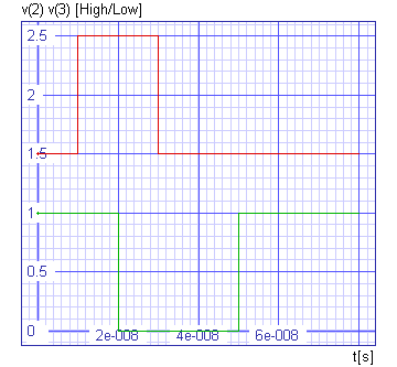
Rise and fall delays for an inverter. The input signal is red and the output signal is green. Rise delay is set to 20ns and fall delay to 10ns.
The signal is at the end converted from digital to analog with a digital-to-analog node bridge. These bridges
have parameters for output voltages that are produced for all three logic levels (out_low, out_high and
out_undef), an input_load parameter with the same meaning as with other logic gates and a rise/fall time
parameters for the output voltage (t_rise, t_fall).
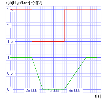
Rise and fall times for the digital-to-analog node bridge. The input signal is red and the output signal is green. Rise time is set to 20ns and fall time to 10ns.
In order to observe the state of a digital node its value must be converted from digital to analog using a digital-to-analog node bridge and then observed as analog voltage.
.cm library files included with SPICE OPUS
There are 4 .cm files provided with SPICE OPUS. They contain an extensive set of CMs and UDNs for analog and event-driven simulation. To learn more about these code models and UDNs take a look at their sources in lib/cmsource. Especially the .ifs files contain many valuable information about the code models.
analog.cm
| Name | CM or UDN | Description |
|---|---|---|
| climit | CM | Controlled limiter block. The limits are controlled by two inputs (one for high limit and one for low limit). Offset and gain can be specified for the input. The linear range has a lower limit that is set by the user (limit_range parameter). limit_range can be specified either as an absolute range (default) or percent of difference between upper and lower limit. Smoothing is used in the transition from linear part to limiting in order to avoid convergence problems. Smoothing is specified by upper_delta and lower_delta parameters. |
| divide | CM | A two-quadrant analog divider. It has a numerator and a denominator input and an output. Offset and gain can be specified for both inputs and the output. The denominator is limited to a value above zero specified as den_lower_limit. The limit is approached through a quadratic smoothing function. The domain of this function can be specified as a fraction of the lower limit (default) or as an absolute value. |
| d_dt | CM | Differentiator. Output offset and gain can be specified. Output can be limited if out_lower_limit or out_upper_limit parameters are specified. The incremental value of output at which smoothing occurs (when limitng is used) is specified by the limit_range parameter. Do not use this model in a feedback loop in order to provide an integration function since it doesn't check for truncation errors. Use the integrate model instead. |
| gain | CM | A simple gain block. Its parameters are gain, input_offset and output_offset. |
| hyst | CM | A hysteresis buffer block. The in_low and in_high specify the center value around which the block operates. Output values are limited to out_upper_limit and out_lower limit. The lower transition slope starts at in_lower-hyst and ends at in_upper-hyst. The upper transition slope starts at in_lower+hyst and ends at in_upper+hyst. Smoothing is performed at the transition from slope to limiting. The smoothing is specified by the input_domain parameter and can be given either as an absolute value or as percent of difference between in_high and in_low. The type of the input_domain parameter is defined by the fraction boolean parameter. |
| ilimit | CM | A current limiter block. This is actually a high level model for an opamp. The input signal is taken from the in port. in_offset and gain are applied to this voltage giving veq. Then it is limited between values from the pos_pwr and neg_pwr ports. If the result is greater than the out port voltage, a sourcing current flows from the output pin. In the opposite case a sinking current flows into the output pin. The output resistance depends on the polarity of the current flow (r_out_source, r_out_sink). The source/sink current is limited by the i_limit_source and i_limit_sink parameters. The output current is reflected on the pos_pwr/neg_pwr ports as current. v_pwr_range controls the smoothing just before veq rises above pos_pwr or falls below neg_pwr. i_source_range and i_sink_range specify the range at which the sourcing/sinking current is smoothed. For veq-vout below r_out_domain and above -rout_domain the output resistance is interpolated between r_out_source and r_out_sink. |
| int | CM | Integrator block. Input offset and gain can be specified. The output can be limited. When the output is limited, the transition to limiting is smoothed in the limit_range below out_upper_limit and above out_lower_limit smoothing is performed. The integrator can be given an output initial condition. |
| limit | CM | Limiter block. input_offset and gain are applied to the input signal and the result is limited to out_lower_limit and out_upper_limit. limit_range specifies the output range in which smoothing occurs. It can be given either as percent or as an absolute value (controlled by the fraction boolean parameter). |
| mult | CM | in_offset array and in_gain array is applied to the vaues from the in vector port. The results are then multiplied together, out_gain is applied and then out_offset is added. The result is sent to the out port. |
| oneshot | CM | The value is taken at the cntl_in port and applied to the cntl_array and pwl_array that describe the pulse width with respect to the cntl_in. The clk_in port triggers the pulse. Trigger level is determined by the clk_trig parameter. pos_edge_trig parameter determines the edge of the clk_in signal that triggers the output pulse when clk_in reaches the clk_trig level. The output starts to rise with rise_delay and rises to its final value after rise_time. pulse_width+fall_delay later the output starts to fall and falls to its initial value after fall_time. The retrig parameter specifies if it is possible to retrigger the output after it was already triggered once. If the clear input is above clk_trig, the state of the oneshot is cleared and it is prepared for a new triggering cycle. |
| pwl | CM | Piecewise linear transfer function. The x and the y array specify the transfer function between input and output. Smoothing is applied to corners in the input_domain range. The smoothing can be given either as a percent or as an absolute value. |
| sine | CM | Controlled sine wave oscillator. The cntl_array and freq_array specify the transformation of input signal into output frequency. A sine signal is generated at the output with the calculated frequency. The out_low and out_high parameters specify the valley and the peak value for the output sine waveform. |
| slew | CM | A simple slew rate follower block. The rise_slope limits the rising slope and the fall_slope limits the fall slope of the output signal. The units for the slope limits are V/s or A/s. |
| square | CM | Controlled square wave oscillator (see sine CM). The cntl_array and freq_array specify the transformation of input signal into output frequency. A square signal is generated at the output with the calculated frequency. The out_low and out_high parameters specify the valley and the peak value for the output waveform. duty_cycle, rise_time and fall_time determine along with the calculated frequency the output waveform. |
| summer | CM | The in_offset array is added to the in vector port inputs. The results are then multiplied with the gains form the in_gain array and added together. The sum is multiplied by out_gain and out_offset is added. The result is sent to the out port. |
| s_xfer | CM | A s-domain transfer function between out port and in port. in_offset and gain are applied to the input signal. The signal is filtered using a s-domain transfer function. The transfer function is described by the num_coeff and den_coeff arrays. The first element of these two arrays is the one that belongs to the highest order in the numerator/denominator s-domain polynomial. Initial conditions can be provided for the integrators using a vector parameter int_ic. The denormalized_freq parameter is used to transform the frequency. For instance a set of coefficients for a low-pass filter with cut-off frequency at 1Hz can be given in num_coeff and den_coeff and then transformed by the CM to a filter with cut-off frequency at 100Hz by setting the denormalized_freq parameter to 100. |
| triangle | CM | Controlled triangle wave oscillator (see sine CM). The cntl_array and freq_array specify the transformation of input signal into output frequency. A triangle signal is generated at the output with the calculated frequency. The out_low and out_high parameters specify the valley and the peak value for the output waveform. duty_cycle parameter specifies the rise time duty cycle for the signal. |
digital.cm
| Name | CM or UDN | Description |
|---|---|---|
| adc_bridge | CM | Analog-to-digital node bridge with vector input and vector output ports. |
| dac_bridge | CM | Digital-to-analog node bridge with vector input and vector output ports. |
| d_and | CM | AND gate with vector input and single output. |
| d_buffer | CM | Single input/single output buffer. |
| d_dff | CM | D-type flip-flop with input, clock, async. set, async. reset, out and inverted out. As parameters you can specify rise_delay, fall_delay, set_delay, reset_delay, clk_delay, initial_state, data_load, clk_load, set_load and reset_load. |
| d_dlatch | CM | D-type latch with input, enable, set, reset, out and inverted out. It has the same parameters as d_dff except that instead of clk_delay it has enable_delay. |
| d_fdiv | CM | Frequency divider. The number of input cycles for high output are set with the high_cycles parameter. The divide factor is set by the div_factor parameter. Output initial count value can also be set using the i_count parameter. |
| d_inverter | CM | Digital inverter. |
| d_jkff | CM | JK-type flip-flop. Similar to d_dff except that instead of one input it has a J and a K input. |
| d_nand | CM | NAND gate with vector input and single output. |
| d_nor | CM | NOR gate with vector input and single output. |
| d_openc | CM | Digital one-bit-wide open collector buffer. |
| d_opene | CM | Digital one-bit-wide open emitter buffer. |
| d_or | CM | OR gate with vector input and single output. |
| d_osc | CM | Controlled digital oscillator. The cntl_in analog input along with the cntl_array and freq_array parameters is used to determine the output signal frequency. duty_cycle parameter determines the output duty cycle. init_phase determines the initial phase of the output signal in degrees. rise_delay and fall_delay specify the delays of the rising and falling edge of the signal. |
| d_pulldown | CM | Generates a RESISTIVE strength ZERO level at the node to which it is connected. |
| d_pullup | CM | Generates a RESISTIVE strength ONE level at the node to which it is connected. |
| d_ram | CM | Random-Access Memory. Ports: data_in and data_out (both vector), adress (vector), write_en, select (chip select), |
| d_source | CM | Digital source. The output sequence is read from a file. |
| d_srff | CM | SR-type flip-flop. Similar to d_jkff except the instead if J and K input it has S and R input. |
| d_srlatch | CM | SR-type latch. Similar to d_dlatch, except that instead of single input it has S and R input. |
| d_state | CM | Digital state machine with vector in, clock, reset and vector out. The state transition table is read from a file. |
| d_tff | CM | T-type flip-flop. Similar to d_dff except that it has a T input instead of a D input. |
| d_tristate | CM | Tristate buffer with input, enable and output. |
| d_xnor | CM | XNOR gate with vector input and single output. |
| d_xor | CM | XOR gate with vector input and single output. |
xtradev.cm
| Name | CM or UDN | Description |
|---|---|---|
| aswitch | CM | Smooth transition analog switch. It is a resistor that varies either logaritmically or linearly between specified values of the controlling input. |
| capacitor | CM | A CM capacitor with voltage inital condition and support for supply ramping. |
| cmeter | CM | A capacitance to voltage convertor that converts the total capacitance seen on its input into output voltage. |
| core | CM | A H-B core model. Current through this model stands for magnetic flux (B*area) and voltage across it for magnetomotive force (H*length). Used in conjunction with the lcouple model for modelling coupled electric and magnetic circuits. It has two modes of operation. In mode 1 it works as a B-H transfer function determined by the H_array and B_array parameters. In mode 2 it operates as a hysteresis block between H and B (see hyst CM). |
| aswitch | CM | Smooth transition analog switch. It is a resistor that varies either logaritmically or linearly between specified values of the controlling input. |
| inductor | CM | A CM inductor with current inital condition and support for supply ramping. |
| lcouple | CM | Inductive coupling. Used in conjunction with the core model. The mmf_out port connects to the magnetic part of the circuit and the l port to the electric part of the curcuit. It has only one parameter: number of turns. |
| lmeter | CM | A inductance to voltage convertor that converts the total inductance seen on its input into output voltage. |
| potentiometer | CM | A potentiometer with two pot connections and a wiper connection. With the parameters the total resistance, wiper position, type (lin, log) and log multiplier (number of decades between wiper position 1 and position 0) can be set. |
| zener | CM | Simple Zener diode model. |
xtraevt.cm (library under construction)
| Name | CM or UDN | Description |
|---|---|---|
| d_to_real | CM | Digital-to-real node bridge with digital enable input. |
| int | UDN | Integer type user defined node. The resolution of conflicting values is done by adding them together and posting the result as the node value. |
| real | UDN | Real type user defined node. The resolution of conflicting values is done by adding them together and posting the result as the node value. |
| real_delay | CM | Real delay block. Delays the real input by one digital input clock period. |
| real_gain | CM | Applies input offset, input gain, output offset and delay to a real signal. |
| real_to_v | CM | Real-to-analog node bridge. |
How to build your own .cm library
A .cm library can contain multiple CMs and UDNs. Look at the sources of the .cm files that come with Spice Opus to see how to create your own .cm library. The cmpath.lst and udnpath.lst files list the names of CMs/UDNs that are included in a .cm library. A .cm library is actually a dynamically loaded library (.dll under Windows, .so under Linux) with a custom file ending (.cm). The dllmain.c file contains the interface to the .cm library. Typically you don't have to edit this file apart form changing the information on the creator of the .cm file (you).
Building the .cm sources (before r294)
For Windows a MSVC solution and project files can be found in the build/win-vstudio-sln-cm and build/win-vstudio-proj directories in the Spice Opus tree.
For Linux Makefiles are available in the src/spiceopus directory of the Spice Opus tree. There is only one main makefile named Makefile.rules. All other makefiles include this file and specify only a minimal amout of information needed for the compilation. There is no need to list the source files because Makefile.rules automatically discoveres and compiles them. Typically you only specify the sub-directories and the target name.
To clean up the sources type
make clean
To compile the sources type
make
To install the compiled .cm files in lib/spiceopus/cm in the Spice Opus tree type
make install
Make sure you have write permission to the directory where Spice Opus is installed.
Building the .cm sources after r294 (Windows)
The build system must be generated with CMake. You need CMake version 3.20.1 or newer. You also need Visual Studio 2015 or newer. Create a directory where the build system will be created. Start a VS2015 x64 Native Tools Command Prompt. Then enter that directory with the cd command and type
cmake -G "NMake Makefiles" -D CMAKE_BUILD_TYPE=Release <sources path>
Then run
nmake
After the .cm files are built, run
nmake install
To generate the build system for the Debug version of the .cm files pass -D CMAKE_BUILD_TYPE=Debug to CMake.
CMake can also generate a VS2015 solution. The solution can build the Release and the Debug version of the .cm files. Create a directory for the solution, start a VS2015 x64 Native Tools Command Prompt, enter the created directory with the cd command, and type
cmake -G "Visual Studio 14 2015 Win64" <sources path>
Now open the generated solution with VS and compile the sources.
Building the .cm sources after r294 (Linux)
You will need CMake 3.13.4 or newer and GNU Make.
Create a directory where CMake will generate the build system, enter it, and type
cmake -G "Unix Makefiles" -D CMAKE_BUILD_TYPE=Release <sources path>
Then run
make
After the .cm files are built, run
make install
To generate the build system for the Debug version of the .cm files pass -D CMAKE_BUILD_TYPE=Debug to CMake.
To load the library, use the cmload Nutmeg command.