10.5.4. Customization example: netlisting MOS devices as subcircuits
In section Using the pyopus.lib library in eeschema the MOS transistors were simulated as builtin SPICE devices (i.e. their names all started with M to indicate this). What to do when your MOS transistors models define them as subcircuits. This is often the case in integrated circuit design where several other parameters that define the parasitics must be specified (like AD, AS, PD, AS, ...). These parameters generally depend on channel dimensions. Therefore MOS transistor models are often defined as subcircuits that automatically compute these parameters from channel dimensions. For our example suppose we have two such subcircuits defined, one for NMOS and one for PMOS. The definition of these two subcircuits can be found in file mosmm.inc.
* Mismatch model of NMOS and PMOS, Spice Opus
*   w, l, m    ... MOS parameters
*   vtmm, u0mm ... normalized mismatch (+1 means +1 sigma)

.subckt nmosmod drain gate source bulk param: w l m=1 vtmm=0 u0mm=0
.param sqrtarea=sqrt(w*l*m)
.param vvt=vtmm*(5e-3*1e-6/sqrtarea/sqrt(2))
.param vu0r=u0mm*(1.04e-2*1e-6/sqrtarea/sqrt(2))
vgmm (gate gate_int) dc={vvt}
m0 (drain gate_int source bulk) nmosmod w={w*(1+vu0r)} l={l} m={m} ad={w*0.18u} as={w*0.18u} pd={2*(w+0.18u)} ps={2*(w+0.18u)} nrs={0.18u/w} nrd={0.18u/w}
.ends

.subckt pmosmod drain gate source bulk param: w l m=1 vtmm=0 u0mm=0
.param sqrtarea=sqrt(w*l*m)
.param vvt=vtmm*(5.49e-3*1e-6/sqrtarea/sqrt(2))
.param vu0r=u0mm*(0.99e-2*1e-6/sqrtarea/sqrt(2))
vgmm (gate gate_int) dc={vvt}
m0 (drain gate_int source bulk) pmosmod w={w*(1+vu0r)} l={l} m={m} ad={w*0.18u} as={w*0.18u} pd={2*(w+0.18u)} ps={2*(w+0.18u)} nrs={0.18u/w} nrd={0.18u/w}
.ends
The file defines two subcircuits named nmosmod and pmosmod that wrap the two
builtin MOS models which are also names nmosmod and pmosmod. Both of them have
5 parameters (W, L, M, VTMM and U0MM). The meaning of VTMM and U0MM will be explained
in section Customization example: generating MOS mismatch parameters. For now we assume they are set to their default
value 0.
To use these two subcircuits we would have to add several Fields to every MOS instance in the Miller OTA schematic. But we can get away with much less work if we alter the netlister behavior with the following netlister.json file.
{
        "Mapping": [
		[
			null, "PMOS",
			{
				"Parameters": [ "w", "l", "m", "vtmm", "u0mm" ],
				"OutPattern": "#REF() (#PINS()) #MODEL() #PARAM() #PNV() #PV(Specification)",
				"SpiceDevice": "subcircuit",
				"PinMap": [ 1, 2, 3, 4 ],
				"NamePrefix": "X",
				"ValueField": null
			}
		],
		[
			null, "NMOS",
			{
				"Parameters": [ "w", "l", "m", "vtmm", "u0mm" ],
				"OutPattern": "#REF() (#PINS()) #MODEL() #PARAM() #PNV() #PV(Specification)",
				"SpiceDevice": "subcircuit",
				"PinMap": [ 1, 2, 3, 4 ],
				"NamePrefix": "X",
				"ValueField": null
			}
		]
	]
}
This netlists the MOS transistors as subcircuits. The name prefix is now X instead
of M. The list of parameters includes parameters of the above defined subcircuits
instead of those available for builtin MOS devices. Most importantly, the netlisting
pattern is changed to that of a subcircuit.
If we netlist the miller.sch schematic again we get the following netlist.
*********
* SPICE OPUS netlister for KiCad
* (c)2017 EDA Lab FE Uni-Lj
*
* Netlister : KiCad -> Spice Opus
* Config    : /home/arpadb/pytest/demo/kicad/04-subcktmodel/netlister.json
* Source    : /home/arpadb/pytest/demo/kicad/04-subcktmodel/miller.sch
* XML input : /home/arpadb/pytest/demo/kicad/04-subcktmodel/miller.xml
* Output    : /home/arpadb/pytest/demo/kicad/04-subcktmodel/miller.inc
* Date      : Thu 09 Nov 2017 06:12:27 PM CET
* Tool      : Eeschema 4.0.5+dfsg1-4
* Sheet 1   : / -- miller.sch
*********

.subckt miller inp inn out vdd vss

* Sheet: /
xm2 (net001 net004 vss vss) nmosmod param: w=79.46u l=1.91u m=1
xm1 (net004 net004 vss vss) nmosmod param: w=20.80u l=0.32u m=1
xm3 (out net004 vss vss) nmosmod param: w=60.23u l=0.32u m=1
xm6 (net002 net002 vdd vdd) pmosmod param: w=90.43u l=3.92u m=1
xm7 (net003 net002 vdd vdd) pmosmod param: w=90.43u l=3.92u m=1
xm8 (out net003 vdd vdd) pmosmod param: w=83.01u l=0.20u m=2
i1 (vdd net004)  dc=100u
r1 (out net005) r=67.6k
c1 (net005 net003) c=13.5p
xm4 (net002 inn net001 vss) nmosmod param: w=67.29u l=3.97u m=1
xm5 (net003 inp net001 vss) nmosmod param: w=67.29u l=3.97u m=1

.ends
For the simulation we must include the two subcircuit definitions from mosmm.inc.
We do that in the top level schematic topdc.sch.
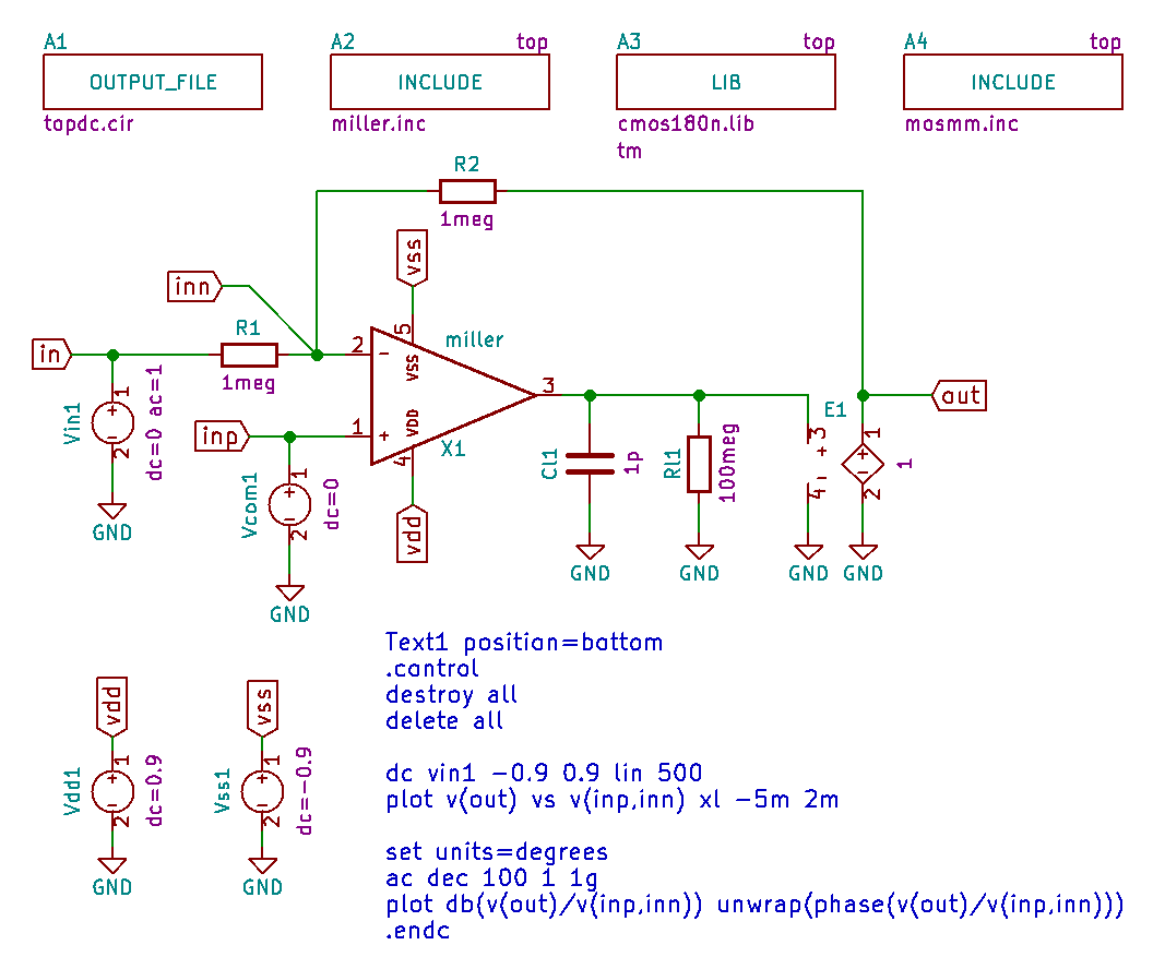
Top level circuit definition that included the mosmm.inc file.
Demo files for this section can be found here.